
Stripe patterns in planar cells
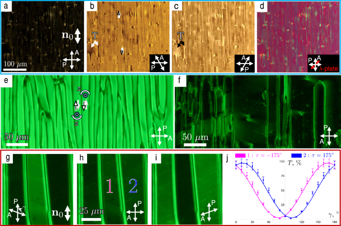
The planar cells in the N and SmZA phases show homogeneous textures with the molecular director \(\hat \) parallel to the photoinduced apolar easy axis \(\pm {\hat{}}_=(0,\pm 1,0)\). Here and in what follows, we use the Cartesian coordinates (x, y, z) in which the y-axis is the direction of the anchoring and the z-axis is normal to the film. Upon cooling, the texture remain homogeneous for about (4−8) °C below the SmZA-NF transition point, depending on the cell thickness. Thin cells, h P = P(0, ± 1, 0) for (6−8) °C, after which they split into a lattice of UDs elongated along \({\hat{{ }}}_\), each of width on the order of 10 μm, Fig. 1a–d. When \({\hat{{{ }}}}_{0}\) is parallel to one of the polarizers, the UDs are practically extinct between two crossed polarizers, Fig. 1a, and their optical retardance equals that of the optical compensator when the latter is inserted between the sample and the analyzer, Fig. 1d. The textures observed with polarizers uncrossed counterclockwise, Fig. 1b, and clockwise, Fig. 1c, differ little from each other. One concludes that P in UDs aligns along \({\hat{{{{\bf{n}}}}}}_{0}\) and their polarity alternates from P = P0(0, 1, 0) in one domain to P = P0(0, −1, 0) in the next. There are only few regions, marked with a letter T in Fig. 1b, c, in which the textures with uncrossed polarizers do differ, which suggests a twist of P along the z-axis.

a A polarizing optical microscopy texture of uniform domains (UDs) in a thin NF cell, h = 0.7 μm (temperature T = 55 °C) with bidirectional anchoring indicated by the white double arrow. b, c The same, counterclockwise and clockwise uncrossing of analyzer and polarizer, respectively. Pairs of parallel arrows in (b) illustrate that P does not change along the z-axis normal to the cell but alternates from one UD to the next along the x-axis. d The same, observation with an optical compensator; the slow axis is along the red double arrow. Most domains are uniform in (a–d), with the exception of small areas labeled with a letter T, indicating a π-twisted region. e Polarizing optical microscopy texture of a thick NF cell, h = 5 μm (T = 60 °C). Light transmission indicates that the sample is split into π-twisted domains (π-TDs), shown schematically by two antiparallel arrows that twist by π around the z-axis. f Domains are suppressed when DIO is doped with 0.5 wt.% of an ionic fluid BMIM-PF6, shown for a cell with h = 4.0 μm (T = 43 °C). g–i The twisted polarization in the π-TDs is readily recognized by observing the textures with uncrossed (g, i) and crossed (h) polarizers, for a cell with h = 4.0 μm (T = 60 °C). Textures (e–i) are captured using a green interferometric filter with a center wavelength λ = 532 nm and 1 nm bandwidth. j Theoretical fits (lines) to light transmission data (points) measured through small localized regions in the two domains highlighted in (h) as a function of the angle γ between the polarizers. Fits yield twist angles τ = ± 175° (see Methods) in the two adjacent domains. Error bars are standard deviations of the intensity fluctuations.
Thick cells, h > 2 μm, show a very different behavior. Below 62 °C, they develop a stripe pattern of π-twisted domains (π-TDs), recognized by the absence of light extinction when viewed between two crossed polarizers, one of which is along \({\hat{{{{\bf{n}}}}}}_{0}\), as seen in Fig. 1e. This NF texture is similar to the previously studied TDs with alternating left-handed and right-handed twists in cells in which one plate sets a unipolar alignment of P and the other is azimuthally degenerate10.
The addition of an ionic salt 1-Butyl-3-methylimidazolium hexafluorophosphate (BMIM-PF6) suppresses the π-TDs, as the sample is predominantly extinct between the crossed polarizers, Fig. 1f. The added salt also decreases the temperatures of phase transition by ~20 °C, in agreement with previous studies10,13,14. The dependency of a transmitted light intensity on the angle γ between the directions of polarization of the polarizer and analyzer allows one to determine that the twist angle τ between the bottom and top orientation of P in the DIO cell of a thickness h = 4 μm is close to 180°, Fig. 1g–j.
Note that the domain structures presented in Fig. 1 are different from the recently described splay and double-splay domain structures that form in the material RM734 above the phase transition to the NF14,15. These splay domain structures are optically discernable when the material is exposed to an ionic fluid14 or an ionic polymer15. The splay domains above the NF temperature range are attributed to the flexoelectric effect, which favors the splay of molecules with head-tail asymmetry14,15. In the NF phase, this flexoelectricity-triggered splay is suppressed by the space charge that accompanies divergence of P14. As a result, the domain structures in the NF phase, Fig. 1, are different from the domain structures reported in refs. 14,15. Thus, in what follows, we disregard the flexoelectric effect.
Pie slices in cells pre-patterned with a +1 radial splay defect
The radial patterns of the +1 defect in the N and SmZA phases demonstrate smooth splay deformation of the director. In the NF phase, the textures show domains of two types: The first are pie slices, or splay domains (SDs), with P parallel or anti-parallel to the radial direction \(\hat{{{{\bf{r}}}}}\), pointing either away from the core of the +1 defect at \(\hat{{{{\bf{r}}}}}=0\) or towards it, as shown in Fig. 2a, b. As established by polarizing microscopy, within each SD, P does not twist along the z axis, except perhaps within the domain walls that separate sectors of antiparallel P, similar to the UDs in the planar cells. The second type are π-TDs, similar to the π-TDs in the planar cells: P twists around the z axis by τ ≈ 180°, as shown in Fig. 3.

a A polarizing optical microscopy texture (recorded in a monochromatic light using a green filter with 532 nm wavelength and 1 nm bandwidth) of an NF cell with thickness h = 2 μm, T = 55 ∘C, and cooling rate 0.1 ∘C/min. The parallel arrows show the parallel polarizations at the bottom and top plates, with π flips from one splay domain (SD) to the next along the azimuthal direction. b Similar cell but recorded under white light, h = 2 μm, T = 55 ∘C, and cooling rate 5∘C/min. c, d Number of domains as a function of distance R from the defect core for cell thicknesses h = (1 − 16) μm, cooling rates 0.1 ∘C and 5 ∘C, respectively. e Number of domains versus h measured at different distances R from the defect core, cooling rate 0. 1 ∘C/min. Filled symbols and solid lines correspond to the total domain count, while open symbols and dashed lines correspond to the number of π-TDs. f The h-dependence of the number of domains, cooling rate 5 ∘C/min. Error bars in (c–f) are estimates of uncertainties in the domain count in the sample. g Fraction of TDs as a function of the cell thickness h measured at different distances R from the defect core; cooling rate 0.1 ∘C/min. h Radial structure with no domains in a thin cell, h = 1 μm (T = 50 ∘C), imaged using the Microimager PolScope with the ticks showing the director field \(\hat{{{{\bf{n}}}}}(x,y)\). The thin blue line of decreased retardance is a domain wall separating the +1/2 defects that split from the central +1 splay pattern.

a A polarizing optical microscopy texture (recorded in a monochromatic light using a green filter with 532 nm wavelength and 1 nm bandwidth) of an NF in a cell of the thickness h = 5.5 μm (DIO, temperature T = 60 ∘C). The curved white arrow shows the direction of polarization twist and the anti-parallel arrows indicate the π-twist of P between the top and bottom plates. b Schematic of the polarization P (green arrow) performing a π-twist between the bottom and top cell surfaces (orange). c Fitting the dependence of transmitted light intensity [through a small region in a domain like the red rectangle in a] on the angle γ between the polarizers yields the twist angle τ ≈ 180∘ for samples of different thickness in the range 3 μm h π-twist (see Methods). The error bars are the standard deviations of light intensity fluctuations in the measured small regions.
Thick cells, h > 6 μm, upon cooling below 61 °C, show exclusively π-TDs, Fig. 2e, g. Cells of an intermediate thickness, 1 μm h π-TDs and SDs, Fig. 2e, g. Structures in cells with h ≤ 1 μm are either uniformly radial, Fig. 2h, or show a few SDs. In all of these cases, there is splay deformation originating from the +1 central vortex and the SDs and π-TDs terminate in a complex manner near this central defect region (i.e., at the tips of the pie slices), as seen in Fig. 2b. Thus, when comparing these samples to our theoretical results below, we will focus on the region away from this complex region, out at distances R ≈ 100 μm from the defect center where the sectors do not terminate but where we still find substantial splay deformation and, consequently, the presence of bound charge.
In thin cells, 1 μm h A-NF transition point. The thickness dependency of the temperature at which the domains appear can be qualitatively explained by the temperature dependence of the polarization magnitude P0 which increases from about P0 = 3.4 × 10⁻² C/m2 to P0 = 4.6 × 10⁻² C/m22 as the temperature decreases following the SmZA-NF transition; the bound charge effects leading to the domains might be weaker than the stabilizing surface anchoring and ion screening.
The addition of either a π-TD or SD domain increases the effective charge of the central defect as the polarization orientation will twist by an additional factor of 2π for each pie slice in the domain configuration. The central +1 defect in the pattern, then, breaks up into a complex arrangement where all of the pie slice corners merge together. When there are no sectors, such as in thin cells with h ~ 1 μm, the +1 defect splits into two +1/2 defect cores separated by a domain wall, as illustrated in Fig. 2h with a thin blue line of a somewhat smaller retardance (~160 nm versus ~210 nm in the far-field). This result indicates that there is no melting of the ferroelectric order (in which case the domain wall will be absent) nor significant escape into the third dimension (in which case the central part would have significantly lower retardance). In a regular nematic N, the +1 defect in the center would break up into disclination lines or contain an escaped structure16. The absence of the escape into the third dimension in the NF is also evident in other textures in Figs. 2–4. This is not surprising since, in an NF, such an escape of P along the normal to the cell would either deposit surface charges at the bounding plates or create additional splay with an accompanying bulk space charge. Note that even in a paraelectric N, a +1 defect prefers to split into a pair of +1/2 defects when the cell is sufficiently thin (see refs. 16,17,18).

A polarizing optical microscopy texture (recorded in a monochromatic light using a green filter with 532 nm wavelength and 1 nm bandwidth) of the NF phase of, a, pure DIO, T = 50 ∘C and b, DIO doped with 0.5% BMIM-PF6, T = 43 ∘C in cells with radial patterns of the thickness h = 1.9 μm. c Number of domains versus distance to the +1 defect center for pure DIO and DIO doped with BMIM-PF6. Error bars indicate that it was difficult to distinguish about two of the sectors in the two samples.
Within the range of coexistence, the fraction of the SD domains increases as the cell thickness h decreases, Fig. 2e, g. The number of domains increases with the cooling rate, Fig. 2c, d. One potential reason is that for a longer cooling time, the highly polar material absorbs ions from the surroundings, such as glue, BY layer, etc., to screen the bound charge. The ion concentration of free ions in the NF cannot be measured directly by conventional techniques since polarization reorientation reduces the electric field in the NF bulk19. Briefly heating the sample to 120 °C into the N phase and measuring the concentration supports the idea that ion concentration can increase in time: We find c(0) = 5.0 × 10²² ions/m3 at the start of experiment to c(18 hours) = 6.3 × 10²² ions/m3 after 18 h of keeping the sample in the NF phase at 65 °C. The number of domains decreases significantly when DIO is doped with the ionic fluid BMIM-PF6, Fig. 4. At a weight concentration 0.5 wt% of BMIM-PF6, (an ion concentration of 1.5 × 1025 ions/m3 for fully ionized added molecules), the NF phase preserves ferroelectric ordering, as reported by Zhong et al.13.
Theory of twisted cylindrical domains
To begin the theoretical analysis, we first review Khachaturyan’s theoretical prediction from 197520 that NFs may spontaneously develop twisted polarization P domains with a certain period λz. We consider a cylindrical domain with radius R and length h, as shown in Fig. 5. In the absence of twist, a uniform polarization (\({{{\bf{P}}}}={P}_{0}\hat{{{{\bf{x}}}}}\), say) will generate a strong depolarization field due to the accumulation of uncompensated charge on the domain boundary, as shown on the left panel of Fig. 5. The charges can be partially compensated by twisting the direction of P along the cylinder, as demonstrated on the right panel of Fig. 5. Note that this model is an idealization, as the polarization P in a real sample will typically not terminate with any component normal to the boundary, precisely to avoid the accumulation of the bound charge. There will thus likely be a complex deformation of the polarization near such a boundary. Although such configurations are beyond the scope of our analysis, we can use this idealized model to demonstrate the competition between electrostatics and elasticity in a simple way.

A uniform polarization \({{{\bf{P}}}}={P}_{0}\hat{{{{\bf{x}}}}}\) (left panel) incurs an energetic cost due to the uncompensated charges and consequent depolarization field Edep. Instead, the polarization P can twist (right panel) with a certain period λz and create regions of alternating charge, thereby partially mitigating the energetic cost of the depolarization field. This twist is balanced by the elastic cost of the twist.
The NF has a continuously varying polarization vector P ≡ P(r) = P0n(r) within the material, with some fixed magnitude ∣P∣ = P0 and a varying orientation n(r). The bound charge distribution is given by ρ = − ∇ ⋅ P. We can calculate the corresponding (screened) electrostatic energy as
$${F}_{\rho }=\frac{1}{8\pi \epsilon {\epsilon }_{0}}\,\iint \,\frac{\rho ({{{\bf{r}}}})\rho ({{{{\bf{r}}}}}^{{\prime} }){e}^{-\kappa | {{{\bf{r}}}}-{{{{\bf{r}}}}}^{{\prime} }| }}{| {{{\bf{r}}}}-{{{{\bf{r}}}}}^{{\prime} }| }\,{{{\rm{d}}}}{{{{\bf{r}}}}}^{{\prime} }\,{{{\rm{d}}}}{{{\bf{r}}}},$$
(1)
where ϵ is the relative dielectric constant of the material and κ ≡ 1/λD is the (inverse) Debye screening length as derived in the Debye–Hückel approximation. We have \(\kappa \approx \sqrt{n}\,e/\sqrt{\epsilon {\epsilon }_{0}{k}_{B}T}\) for monovalent ions with concentration n, with e the fundamental charge, ϵϵ0 the material permittivity, and kBT the thermal energy. This free energy Fρ can be expressed in Fourier space as
$${F}_{\rho }=\frac{1}{2\epsilon {\epsilon }_{0}}\,\int\frac{| {{{\bf{k}}}}\cdot {\tilde{{{{\bf{P}}}}}}_{{{{\bf{k}}}}}{| }^{2}}{| {{{\bf{k}}}}{| }^{2}+{\kappa }^{2}}\,\,\,\frac{{{{\rm{d}}}}{{{\bf{k}}}}}{{(2\pi )}^{3}},$$
(2)
where \({\tilde{{{{\bf{P}}}}}}_{{{{\bf{k}}}}}\equiv \int\,{{{\rm{d}}}}{{{\bf{r}}}}\,{e}^{-i{{{\bf{k}}}}\cdot {{{\bf{r}}}}}{{{\bf{P}}}}({{{\bf{r}}}})\). Even in cases where ρ(r) vanishes in the bulk, we may get contributions to Fρ due to charges at the boundaries. Note that our expression in Eq. (2) assumes that the screened Coulomb interaction occurs throughout the system, including outside of the domain with nonzero polarization P.
Spatial variations of P will incur elastic energy penalties. The (nematic) elastic energy is given by the Frank form
$${F}_{n}=\int\,{{{\rm{d}}}}{{{\bf{r}}}}\left[\frac{{K}_{1}}{2}{(\nabla \cdot {{{\bf{n}}}})}^{2}+\frac{{K}_{2}}{2}{({{{\bf{n}}}}\cdot (\nabla \times {{{\bf{n}}}}))}^{2}+\frac{{K}_{3}}{2}{({{{\bf{n}}}}\times (\nabla \times {{{\bf{n}}}}))}^{2}\right],$$
(3)
with K1, K2, and K3 the splay, twist, and bend elastic constants, respectively21. Note that, in general, P and n have to be treated separately and are not necessarily colinear. Moreover, the proper order parameter for the nematic portion is a symmetric, traceless tensor Q. The more general starting point for describing the NF is given in, e.g., ref. 22. Here we only look at the competition between elastic distortions of the nematic order and the electrostatic self-interaction, assuming that the nematic order always aligns with P. Any other effects will be incorporated in renormalizations of the constants (e.g., the splay K1 and the dielectric constant ϵ) and we leave a more general analysis for future work. Note also that we are neglecting the saddle-splay elastic contribution which can play a role at sample boundaries or at disclinations23. In our case, we will have strong anchoring conditions and any singularities will occur at polarization domain boundaries, which we will treat by introducing a phenomenological description of the energetic cost for domain wall formation, which may include effects from the saddle-splay.
We look at P configurations of the form:
$${{{\bf{P}}}}={P}_{0}(\cos [\phi (z)],\sin [\phi (z)],0)\Theta_R (x,y),$$
(4)
where 0 ≤ z ≤ h, ϕ(z) is the polar angle of the P orientation, and ΘR(x, y) = 1 whenever x2 + y2 ≤ R and ΘR(x, y) = 0 otherwise. This means that we expect to have uncompensated charges at the cylinder boundary, as shown in Fig. 5. We now assume without loss of generality that the angle ϕ(z) is a periodic function with some period 2π/kz which might tend toward infinity:
$$\phi (z)={k}_{z}z+\psi (z),$$
(5)
where ψ(z) = ψ(z + 2π/kz). We may expand the phase factor associated with this angle as
$${e}^{i\phi (z)}={e}^{i{k}_{z}z}{\sum}_{m=-\infty }^{\infty }{A}_{m}{e}^{i{k}_{z}mz},$$
(6)
where Am are complex Fourier coefficients satisfying
$${\sum}_{m=-\infty }^{\infty }{A}_{m}{A}_{m-n}^{*}={\delta }_{n},$$
(7)
with δn = 1 for n = 0 and δn = 0 otherwise. Provided we have a thick sample with h ≫ λD, we substitute Eqs. (4) and (6) into Eq. (2) and find that
$${F}_{\rho }=\frac{\pi {P}_{0}^{2}{R}^{2}h}{2\epsilon {\epsilon }_{0}}\,{\sum}_{n=-\infty }^{\infty }{I}_{1}({\alpha }_{n}){K}_{1}({\alpha }_{n})\left[{A}_{n}^{2}+{({A}_{n}^{*})}^{2}\right],$$
(8)
where \({\alpha }_{n}\equiv \,R\sqrt{{[{k}_{z}(n+1)]}^{2}+{\kappa }^{2}}\) and I1(α), K1(α) are the modified Bessel functions of the first and second kind, respectively. It is worth noting that I1(α)K1(α) is a monotonically decreasing function of α, meaning that the electrostatic energy favors large values of αn ~ kz.
Given the ansatz in Eq. (4) and ignoring any elastic deformation or anchoring energy at the cylinder boundary, only the twist term proportional to K2 contributes to the elasticity and we find
$${F}_{n}=\frac{\pi {K}_{2}{k}_{z}^{2}{R}^{2}h}{2}+\frac{\pi {K}_{2}{R}^{2}h}{2{\lambda }_{z}}\,\,\int_{0}^{{\lambda }_{z}}{{{\rm{d}}}}z\,{\left(\frac{d\psi }{dz}\right)}^{2}.$$
(9)
We may now move to Fourier space by making use of the expansion in Eqs. (6) and (7). We find that
$${F}_{n}=\frac{\pi {R}^{2}h{K}_{2}{k}_{z}^{2}}{2}\left[1+{\sum }_{n=-\infty }^{\infty }{n}^{2}| {A}_{n}{| }^{2}\right],$$
(10)
which is minimized for kz → 0. Higher order modes An with ∣n∣ > 0 cost more elastic energy. This is less obvious for the electrostatic interaction in Eq. (8), but Khachaturyan argues on general grounds20 that there is a stable free energy minimum with An = 0 for all ∣n∣ > 0.
Looking at solutions with just the n = 0 mode, we find that the total free energy is given by
$$F={F}_{n}+{F}_{\rho }=\frac{\pi {R}^{2}h}{2}\left[\frac{{P}_{0}^{2}{I}_{1}({\alpha }_{0}){K}_{1}({\alpha }_{0})}{\epsilon {\epsilon }_{0}}+{K}_{2}{k}_{z}^{2}\right],$$
(11)
where \({\alpha }_{0}=R\sqrt{{k}_{z}^{2}+{\kappa }^{2}}\) and \({\sum }_{n}| {A}_{n}{| }^{2}={A}_{0}^{2}={({A}_{0}^{*})}^{2}=1\) from Eq. (7). The total free energy in Eq. (11) now can be minimized with respect to kz for α0, R/λD ≫ 1 [so that \({I}_{1}({\alpha }_{0}){K}_{1}({\alpha }_{0})\approx {(2{\alpha }_{0})}^{-1}\)]. We find a minimum free energy at \({k}_{z}={k}_{z}^{*}\), which corresponds to a preferred pitch \({\lambda }_{z}\equiv 2\pi /{k}_{z}^{*}\) that reads
$${\lambda }_{z}=2\pi {\left[\frac{{P}_{0}^{4/3}}{{(4{K}_{2}R\epsilon {\epsilon }_{0})}^{2/3}}-{\kappa }^{2}\right]}^{-1/2}.$$
(12)
Substituting in reasonable values ϵ = 10, P0 = 4.4 × 10⁻² C/m2, K2 = 10 pN, and R = 100 μm, we find a pitch of λz ≈ 0.4 μm assuming no screening (κ = 0) and increasing with increasing κ. This result is consistent with the previously reported data10 and with the observation that twists disappear in our thinnest cells [see Fig. 1a–c]. Note, however, that λz in the considered model of an infinitely long cylinder cannot be compared directly to the experimental data obtained in Fig. 1 for flat planar samples of large area since the model does not account for the anchoring effects at the lateral surface of the cylinder. In the experiments, the azimuthal anchoring at the top and bottom plates will typically force the sample to adopt either a uniform structure or a twist by π from the top to bottom of the cell, as discussed below.
This result for λz was also recently found by Paik and Selinger using a different analysis24. Note that, due to screening, the twisted state occurs only when the concentration of ions is below some critical value:
Given the reasonable parameters mentioned above and T = 350 K, we find c* ≈ 5 × 10²¹ ions/m3, which is less than the concentration of ions measured in the N phase, c = (5 − 6) × 1022 ions/m3. However, the experimental data obtained in the N phase might not be representative of the concentration of ions in the NF phase. Also, our analysis so far has not taken into account the cell boundary conditions. Nevertheless, the theoretical estimate appears to be consistent with the experiments in which the TDs disappear when DIO is doped with the ionic fluid BMIM-PF6 [see Fig. 1f], which could increase the concentration of ions by orders of magnitude.
Critical cell thickness for π-twists
We now consider an NF confined to a cell with certain imposed nematic orientation n0 at the top and bottom of the cell, as in the samples shown in Fig. 1 with strong anchoring. There is a critical thickness h* for which we get twisted domains if h > h* and domains with uniform P orientation for h h*. When h > h*, the sample thickness h will set the periodicity of the twist along the z direction (see Fig. 1e–j).
We can calculate the critical thickness h* by considering a square domain with dimension L. We assume that P remains in the xy plane and that P runs along \(\hat{{{{\bf{y}}}}}\) on the top and bottom surfaces. We compare two polarization configurations: a uniform \({{{{\bf{P}}}}}_{{{{\rm{uniform}}}}}={P}_{0}\hat{{{{\bf{y}}}}}\) and a π-twisted \({{{{\bf{P}}}}}_{\pi -{{{\rm{twist}}}}}={P}_{0}\sin (\pi z/h)\hat{{{{\bf{x}}}}}+{P}_{0}\cos (\pi z/h)\hat{{{{\bf{y}}}}}\), with all polarizations vanishing outside of the region − L/2 x, y L/2 and 0 z h. The Fourier transforms are
$$\left\{\begin{array}{l}{\tilde{{{{\bf{P}}}}}}_{{{{\rm{uniform}}}}}=\frac{8{P}_{0}\sin \left(\frac{{k}_{z}h}{2}\right)\sin \left(\frac{{k}_{x}L}{2}\right)\sin \left(\frac{{k}_{y}L}{2}\right)\hat{{{{\bf{y}}}}}}{{k}_{x}{k}_{y}{k}_{z}{e}^{ih{k}_{z}/2}}\hfill \\ {\tilde{{{{\bf{P}}}}}}_{\pi -{{{\rm{twist}}}}}=\frac{8{P}_{0}h\sin \left(\frac{{k}_{x}L}{2}\right)\sin \left(\frac{{k}_{y}L}{2}\right)\cos \left(\frac{h{k}_{z}}{2}\right)[\pi \hat{{{{\bf{x}}}}}+ih{k}_{z}\hat{{{{\bf{y}}}}}]}{{k}_{x}{k}_{y}[{\pi }^{2}-{h}^{2}{k}_{z}^{2}]{e}^{ih{k}_{z}/2}}\quad \end{array}\right..$$
(14)
Substituting Eq. (14) into Eq. (2) and assuming that Lκ ≫ 1 (strong screening or large sample size) yields the dipolar energy
$${F}_{\rho }=\left\{\begin{array}{ll}\frac{Lh{P}_{0}^{2}}{\epsilon {\epsilon }_{0}\kappa }\quad &{{{\rm{for}}}}\,{\tilde{{{{\bf{P}}}}}}_{{{{\rm{uniform}}}}}\\ \frac{Lh{P}_{0}^{2}}{4\epsilon {\epsilon }_{0}\kappa }\quad &{{{\rm{for}}}}\,{\tilde{{{{\bf{P}}}}}}_{\pi -{{{\rm{twist}}}}}\end{array}\right..$$
(15)
The electrostatic energy cost of the polarization configuration gets a four-fold decrease from the π-twist along the z-axis.
The π-twisted configuration incurs an elastic energy penalty given by Fn = K2L2π2/(2h), which follows from substituting \({{{{\bf{n}}}}}_{\pi -{{{\rm{twist}}}}}=\sin (\pi z/h)\hat{{{{\bf{x}}}}}+\cos (\pi z/h)\hat{{{{\bf{y}}}}}\) into the Frank free energy, Eq. (3). The balance between elastic and electrostatic energies yields a critical thickness
$${h}^{*}=\frac{\pi }{{P}_{0}}\sqrt{\frac{2\epsilon {\epsilon }_{0}\kappa {K}_{2}L}{3}}.$$
(16)
Even for large domains with L ≈ 1 cm, we find a small h* ≈ (0.2 − 2) μm, for a wide range of screening lengths λD = κ−1 ≈ (0.01 − 1) μm. In the experiments, we find that essentially all domains are twisted for thicknesses h > 2 μm, consistent with this result. Confinement can induce chirality (twist) in solid state ferroelectrics, as well, especially in nanostructured materials25,26, although intrinsically chiral solid ferroelectrics are also possible.
Model of stripe domain patterns
The domains in Fig. 1 are reminiscent of structures found in thin films of solid, uniaxial ferroic materials27, where the polarization P forms stripes of alternating orientation (although the polarization typically has components perpendicular to the film surface, unlike the NF which has P parallel to the xy plane)28,29. The stripes in solid ferroics are generated to mitigate the depolarization field30,31. Similar striped patterns appear in ferromagnetic crystals, with the patterns analyzed 90 years ago by Landau and Lifshitz32.
Consider a thin, square cell with thickness h and square cross section with area Axy = L2, where L = Lx = Ly is the linear extent of our sample. The basic idea, also discussed in detail by Kittel for solid ferromagnetic materials33, is that the dipolar energy density fρ = Fρ/Axy per area of the cell will scale approximately as fρ ∝ λx, with λx the stripe size for stripes running along the y-axis, say. Meanwhile, the introduction of alternating domains of P will incur a cost due to the domain walls. There will be approximately 2L/λx domain walls in the sample, so the associated free energy density will scale according to fdw ∝ 1/λx. There should be an optimal value of λx which balances the two energy densities fdw and fρ.
Let us analyze the optimal wavelength λx by assuming that we have very strong anchoring so that each stripe satisfies the bidirectional boundary conditions at the cell surface, as illustrated in Fig. 6a. One possibility, illustrated in Fig. 6a, is that adjacent domains are of opposite chirality. The corresponding polarization field Pstripe for such a configuration reads
$${{{{\bf{P}}}}}_{{{{\rm{stripe}}}}}=\frac{4{P}_{0}}{\pi }\,{\sum}_{n=1}^{\infty }\,\frac{1}{n}\,\sin \left(\frac{\pi n}{2}\right)\cos (n{q}_{x}x)\cos \left(\frac{\pi z}{h}\right)\hat{{{{\bf{y}}}}}+{P}_{0}\sin \left(\frac{\pi z}{h}\right)\hat{{{{\bf{x}}}}},$$
(17)
where qx = 2π/λx is the wavevector associated with the stripe wavelength λx (see red double arrow in Fig. 6a). The summation over n is the mode expansion of a square wave, so that we have a rapid reorientation of P from \(+{P}_{0}\hat{{{{\bf{y}}}}}\) to \(-{P}_{0}\hat{{{{\bf{y}}}}}\) at the top and bottom of the cell (z = 0, h), as illustrated in Fig. 6a.

a Schematic of a possible polarization direction in the striped domains with characteristic wavelength λx, with the anchoring nematic direction n0 indicated on the top and bottom surfaces. The gray surfaces separating the blue and green domains could be either disclination lines, solitons, of fixed-width domain walls spanning the entire cell height h. b Dimensionless free energy [Eq. (19)] of the striped domain configuration, taking into account both the electrostatic energy contribution and the energy of domain walls (captured by the parameter λdw). We see that there is a minimum at a certain κλx, indicating that the striped configuration is favorable. We show the energy for various values of the dimensionless parameter \(\kappa {\lambda }_{{{{\rm{dw}}}}}\sqrt{L/h}\) discussed in the text.
A sudden jump in the polarization (\(\pm {P}_{0}\hat{{{{\bf{y}}}}}\) in Fig. 6a) is unrealistic and the detailed structure near the flip (gray surfaces separating the green and blue arrows in Fig. 6a) could take a variety of forms including disclination line pairs, a solitonic structure, or a fixed-width domain wall, as discussed in more detail below. We assume here that this region does not significantly influence the electrostatic contribution to the energy, instead contributing to the elastic cost of the polarization domain. We also assume that the striped configuration has some lateral extent 0 x, y L, where L is some integer multiple of λx, for simplicity. Although the system is overall charge neutral, there will be regions of charge at the boundary of the domains along the x, y directions where the polarization arrows terminate, creating depolarization fields.
We substitute the Fourier-transformed Eq. (17) into Eq. (2) to find the dipolar energy of this configuration, again assuming a screened Coulomb interaction everywhere with a screening length κ−1. We find, for large sample sizes Lκ ≫ 1, that
$${F}_{\rho } =\frac{64{P}_{0}^{2}}{{\pi }^{3}\epsilon {\epsilon }_{0}}\,\int\frac{{\cos }^{2}(\frac{z}{2}){\sin }^{2}(\frac{xL}{2h}){\sin }^{2}(\frac{yL}{2h})}{({x}^{2}+{y}^{2}+{z}^{2}+{h}^{2}{\kappa }^{2}){[{\pi }^{2}-{z}^{2}]}^{2}}\left[\frac{{x}^{2}{z}^{2}}{{\pi }^{2}h}{\left[{\sum }_{n=1}^{\infty }\frac{{h}^{2}{\lambda }_{x}^{2}\sin (\frac{\pi n}{2})}{n({\lambda }_{x}^{2}{x}^{2}-4{\pi }^{2}{n}^{2}{h}^{2})}\right]}^{2}+\frac{{h}^{3}{\pi }^{2}}{16{y}^{2}}\right]\\ {{{\rm{d}}}}x\,{{{\rm{d}}}}y\,{{{\rm{d}}}}z \approx \frac{{h}^{2}L{P}_{0}^{2}}{{\pi }^{3}\epsilon {\epsilon }_{0}}\,\left[\int_{-\infty }^{\infty }{{{\rm{d}}}}z\,\frac{{\pi }^{4}{\cos }^{2}(\frac{z}{2})}{{\sqrt{{z}^{2}+{h}^{2}{\kappa }^{2}}[{\pi }^{2}-{z}^{2}]}^{2}}+\frac{2\pi {\lambda }_{x}}{h}{\sum }_{n=1}^{\infty }\,\frac{{\sin }^{2}\left(\frac{\pi n}{2}\right)}{{n}^{2}\sqrt{{(2\pi n)}^{2}+{(\kappa {\lambda }_{x})}^{2}}}\right].$$
(18)
As long as the screening contribution in the sum in Eq. (18) is negligible (λxκ ≲ 1), then the electrostatic energy Fρ grows with λx.
The nature of the domain walls may be complex due to the twist in the polarization P. Experiments indicate that the domain wall may consist of surface disclination lines, with complex elastic distortions in the bulk near the disclinations34,35. In addition, these walls will tend to have vanishing divergence of the polarization P, so we expect no bound charges at the wall locations4,36. An estimate for the energy of the wall (per unit length) due solely to disclinations would be \({f}_{\pi }^{{{{\rm{disc}}}}}\approx 2K\), with K an elastic constant. Another possibility is that the domain wall is a solitonic, Bloch wall structure with an energy governed by the anchoring conditions, which we may call a π-wall/soliton as P flips by 180° across the wall7. The energy per unit length of one such π-soliton is given by \({f}_{\pi }^{{{{\rm{soliton}}}}}\approx 2\sqrt{2KhW}\), where K is an elastic constant, W is the anchoring strength, and h is the cell thickness. A third possibility is that the energy of the wall is proportional to the cell thickness, which may occur if the elastic distortion of the wall extends across the entire thickness h, which may occur for thin cells, so that \({f}_{\pi }^{{{{\rm{wall}}}}}\approx Kh/{\lambda }_{{{{\rm{wall}}}}}\), where λwall is a characteristic width of the wall. We assume here that the characteristic width is independent of h. We will call this case the fixed-width domain wall. In summary, the total elastic cost of domain walls is approximately Fdw ≈ 2fπL2/λx, with fπ either the disclination line pair \(({f}_{\pi }={f}_{\pi }^{{{{\rm{disc}}}}})\), π-soliton (\({f}_{\pi }={f}_{\pi }^{{{{\rm{soliton}}}}}\)), or the fixed-width wall (\({f}_{\pi }={f}_{\pi }^{{{{\rm{wall}}}}}\)) energy density. More complicated possibilities or combinations of these three cases are also possible, but we will focus on just these three cases for simplicity.
Putting it all together, the total energy F = Fρ + Fdw of a striped domain configuration reads
$$\frac{F}{{F}_{0}} =\frac{1}{4}+\frac{\kappa {\lambda }_{x}}{{\pi }^{2}}{\sum }_{n=1}^{\infty }\,\frac{[1-{(-1)}^{n}]}{{n}^{2}\sqrt{{(2\pi n)}^{2}+{(\kappa {\lambda }_{x})}^{2}}}+\,\frac{{(\kappa {\lambda }_{{{{\rm{dw}}}}})}^{2}L}{\kappa {\lambda }_{x}h}\\ \frac{F}{{F}_{0}} \approx \frac{1}{4}+\frac{2\kappa {\lambda }_{x}}{{\pi }^{2}\sqrt{4{\pi }^{2}+{(\kappa {\lambda }_{x})}^{2}}}+\,\frac{{(\kappa {\lambda }_{{{{\rm{dw}}}}})}^{2}L}{\kappa {\lambda }_{x}h},\hskip 3.5pc$$
(19)
where \({F}_{0}=h{P}_{0}^{2}L{(\epsilon {\epsilon }_{0}\kappa )}^{-1}\) is a characteristic free energy and \({\lambda }_{{{{\rm{dw}}}}}={(2{f}_{\pi }\epsilon {\epsilon }_{0})}^{1/2}{P}_{0}^{-1}\) is a characteristic length associated with the domain wall energy density fπ. A similar length was derived some time ago by balancing analogous energetic contributions37. We have made an additional assumption that we can take hκ ≫ 1 in the left-over integration in Eq. (18), which will not change the location of the minimum of F with respect to λx. We plot the dimensionless free energy F/F0 in the first line of Eq. (19) (using first 1000 non-zero terms in the sum) versus κλx in Fig. 6b for various values of \(\kappa {\lambda }_{{{{\rm{dw}}}}}\sqrt{L/h}\), with L the linear extent of the sample. Numerically minimizing the function in Eq. (19) demonstrates that for \(\kappa {\lambda }_{{{{\rm{dw}}}}}\sqrt{L/h} , the free energy curve has a global minimum at a finite value of λx. For larger values, the free energy minimum corresponds to λx → ∞ and a uniform polarization state. In the low screening limit \(\kappa {\lambda }_{{{{\rm{dw}}}}}\ll \sqrt{h/L}\), the preferred wavelength is at
$${\lambda }_{x}^{*}\approx 5.4{\lambda }_{{{{\rm{dw}}}}}\sqrt{\frac{L}{h}}.$$
(20)
Model of pie-slice domains
We now consider the +1 aster defect anchoring condition, with \({{{{\bf{n}}}}}_{0}=\hat{{{{\bf{r}}}}}\) the preferred orientation at the top and bottom cell surfaces. A pure +1 aster defect in the polarization vector, \({{{\bf{P}}}}={P}_{0}\hat{{{{\bf{r}}}}}\), has a corresponding bound charge density distribution
$$\rho (r)=-\nabla \cdot {{{\bf{P}}}}=-\frac{{P}_{0}}{r}.$$
(21)
The distribution of bound charge at the defect is energetically costly, so the NF prefers to reorient along the \(\hat{{{{\boldsymbol{\theta }}}}}\) direction to create a net neutral charge configuration, forming a series of nθ pairs of alternating P domains (with \({{{\bf{P}}}}\parallel \pm \hat{{{{\bf{r}}}}}\)), as shown in Fig. 7a. We also expect a π-twist along the z-direction, but we will neglect the z-dependence for simplicity, focusing on the SDs (see Fig. 2).

a Schematic of the polarization orientation near the cell surface for a cell pre-patterned with a +1 defect. Apart from the domain walls (along the x and y axes and along the dashed line), the polarization P runs along the radial direction \(\hat{{{{\bf{r}}}}}\). The polarization configuration has nθ = 4 pairs of pie-slice sectors of anti-parallel P. b Plot of the rescaled free energy F/F0 in Eq. (26) of a pie-slice pattern with nθ cuts for various values of hκ, with κ the inverse Debye screening length and h the cell thickness. We fix R/h = 100 and ηθ = 30. We see that the Coulomb and elastic energies balance to generate an optimal value of ηθ (the free energy minimum). The dashed vertical line indicates the optimal value, ηθ, in the low screening κ → 0 limit.
Consider the anchoring-imposed splay polarization P configuration in a circular domain of radius R. Far from the defect, as R → ∞, the polarization will be uniform and we expect to see striped domains with the preferred wavelength \({\lambda }_{x}^{*}\) calculated in the previous section. Near the defect, we expect the bound charge distribution in the bulk should play a more significant role. Assuming the polarization remains in the xy plane and does not depend on the distance r from the defect, the form of the polarization vector of such a configuration is
$${{{\bf{P}}}}={P}_{0}\cos [\phi (\theta )]\hat{{{{\bf{r}}}}}+{P}_{0}\sin [\phi (\theta )]\hat{{{{\boldsymbol{\theta }}}}},$$
(22)
where ϕ(θ) describes the polarization orientation away from the \(\hat{{{{\bf{r}}}}}\) direction. The bound charge distribution due to this polarization P is
$$\rho (r,\theta )\approx -\frac{{P}_{0}\cos [\phi (\theta )]}{r},$$
(23)
where we have assumed that ∂θϕ ≪ 1 is negligibly small throughout most of the sample. Regions of opposite (cancelling) charge are created by alternating between ϕ(θ) = 0, π. Note that this approximation will break down close to the +1 defect (the small R region) where all of the domain tips collide. The defect structure there is complex and, even in the absence of domains, the +1 defect splits into two +1/2 defects joined by a domain wall, as discussed previously (see Fig. 2h). We thus consider intermediate values of R ≈ 100 μm when comparing to experiments in the next section.
We perform a single-mode approximation so that \(\cos [\phi (\theta )]\approx \cos ({n}_{\theta }\theta )\). Then, in cylindrical coordinates, the screened Coulomb potential is given by
$$\frac{{e}^{-\kappa | {{{\bf{r}}}}-{{{{\bf{r}}}}}^{{\prime} }| }}{| {{{\bf{r}}}}-{{{{\bf{r}}}}}^{{\prime} }| }=\frac{2}{\pi }{\sum}_{n=0}^{\infty }(2-{\delta }_{n})\cos [n(\theta -{\theta }^{{\prime} })]\,\int_{0}^{\infty }{{{\rm{d}}}}k\,{I}_{n}({x}_{ })\cos [k(z-{z}^{{\prime} })],$$
(24)
where δn = 1 if n = 0 and δn = 0, otherwise. Also, \({x}_{ \ }=\sqrt{{k}^{2}+{\kappa }^{2}}\,{r}_{ \ }\) and r (r>) is the smaller (larger) of the polar distances r and \({r}^{{\prime} }\). Substituting ρ(θ) from Eqs. (23) and (24) into Eq. (1) yields (after some algebra and an identity for the integral of a single modified Bessel function of the first kind Iν(z)38)
$${F}_{\rho }=\frac{32{\pi }^{2}{h}^{3}{P}_{0}^{2}}{\epsilon {\epsilon }_{0}}{\sum}_{m=0}^{\infty }{(-1)}^{m}\int_{0}^{\infty }{{{\rm{d}}}}u\,\frac{{\sin }^{2}(\frac{u}{2})}{{u}^{2}({u}^{2}+{h}^{2}{\kappa }^{2})}\,\int_{0}^{\frac{R}{h}\sqrt{{u}^{2}+{h}^{2}{\kappa }^{2}}}{{{\rm{d}}}}v\,\,{I}_{2m+1+{n}_{\theta }}(v){K}_{{n}_{\theta }}(v),$$
(25)
where Kν(x) is a modified Bessel function of the second kind. The dominant term in the summation is m = 0 and we can make use of the approximations \({I}_{{n}_{\theta }+1}(v){K}_{{n}_{\theta }}(v)\approx v{[4{n}_{\theta }({n}_{\theta }+1)]}^{-1},{(2v)}^{-1}\) for v ≪ nθ and v ≫ nθ, respectively.
The total length of domain wall in the system is 2nθR so that the total elastic cost is Fdw = 2nθRfπ, with fπ the domain wall linear energy density (e.g., either the soliton, the domain wall, or the disclination line pair). We find that the total free energy F = Fρ + Fdw of the pie-slice configuration with nθ cuts (i.e., 2nθ pie slices) reads
$$\frac{F}{{F}_{0}}=\frac{8h{\eta }_{\theta }^{2}}{R}\,\int_{0}^{\infty }{{{\rm{d}}}}u\,\frac{{\sin }^{2}(\frac{u}{2})\,{\Xi }_{{n}_{\theta }}(\frac{R}{h}\sqrt{{u}^{2}+{\kappa }^{2}{h}^{2}})}{{u}^{2}({u}^{2}+{\kappa }^{2}{h}^{2})}+{n}_{\theta },$$
(26)
where F0 = 2Rfπ is a characteristic energy, ηθ = 2πh/λdw is the optimal number of sectors without screening \({\eta }_{\theta }={n}_{\theta }^{*}(\kappa \to 0)\), and \({\Xi }_{{n}_{\theta }}(z)\equiv \int_{0}^{z}{I}_{{n}_{\theta }+1}(z){K}_{{n}_{\theta }}(z)\,{{{\rm{d}}}}z\). The parameter \({\lambda }_{{{{\rm{dw}}}}}\equiv \sqrt{2{f}_{\pi }\epsilon {\epsilon }_{0}}/{P}_{0}\) depends on fπ just as in the stripe case. The plot of Eq. (26) (with numerical evaluation of the integrals) is shown in Fig. 7b. The total free energy exhibits a minimum at a non-zero value of nθ.
We consider two cases: κR ≪ nθ (weak screening) and κR ≫ nθ (strong screening). We find [using asymptotic expansions of the integrals in Eq. (25)39] that, for thin cells compared to the domain size, h ≪ R,
$${F}_{\rho }\approx \frac{{\pi }^{2}h{P}_{0}^{2}}{\epsilon {\epsilon }_{0}}\left\{\begin{array}{ll}\frac{hR}{2{n}_{\theta }} \hfill &\kappa R\, \ll \, {n}_{\theta }\\ \frac{4\pi }{{\kappa }^{2}}\ln \left(\frac{\kappa R}{{n}_{\theta }}\right)\quad &\kappa R\, \gg \, {n}_{\theta }\end{array}\right.$$
(27)
In both cases, this Coulomb energy decreases with increasing nθ, in contrast to the elastic and anchoring energies which will increase proportionally to nθ. We minimize the total free energy F to find the approximate result:
$${n}_{\theta }^{*}\approx \left\{\begin{array}{ll}\frac{2\pi h}{{\lambda }_{{{{\rm{dw}}}}}}\hfill &\kappa R\, \ll \, {n}_{\theta }^{*}\\ \frac{4{\pi }^{3}h}{R{(\kappa {\lambda }_{{{{\rm{dw}}}}})}^{2}}\quad &\kappa R \, \gg \, {n}_{\theta }^{*}\end{array}\right.,$$
(28)
where the large versus small screening conditions have to be checked self-consistently. The value \(2{n}_{\theta }^{*}\) gives the “optimal” number of sectors (i.e., \(\pm \hat{{{{\bf{r}}}}}\) polarization domains).
Quantitative comparisons between models and experiments
A key question is how the domain wall energy density fπ depends on the cell thickness h. One possibility is that the walls are disclination pairs, so that fπ ~ 2K ~ (10 − 1000) pN is independent of the thickness h and is proportional to some combination of elastic constants, here indicated as K. However, for smaller thicknesses h, it is likely that the elastic distortion at the wall extends through the entire cell thickness h and contributes meaningfully to the energy of the domain wall. In this case, we can consider other scalings such as \({f}_{\pi }\propto \sqrt{h},h\) for the soliton and fixed-width domain wall, respectively. These various scalings, then, will change how the characteristic length \({\lambda }_{{{{\rm{dw}}}}}={(2{f}_{\pi }\epsilon {\epsilon }_{0})}^{1/2}{P}_{0}^{-1}\) varies with h, with λdw ∝ h0, h1/4, h1/2 for the disclinations, soliton, and fixed-width domain wall, respectively. These three possibilities are shown in Fig. 8 for both the stripe patterns and the pie-slice sector results, which we consider in more detail below.

Experimental (points) and theoretical predictions (dashed lines) for the number of domains as a function of cell thickness h. In the theoretical models, we fix λD = κ−1 = 10 μm throughout. a TD stripe wavelength \({\lambda }_{x}^{*}\approx 2\langle {w}_{{{{\rm{stripe}}}}}\rangle\) calculated form the average stripe width across a sample with unidirectional, bipolar anchoring. The error bars show the standard deviation over observed stripes. The dashed curves are the wavelengths found by minimizing Eq. (19) over κλx for various models of the domain wall cost, which impacts the characteristic length \({\lambda }_{{{{\rm{dw}}}}}=\sqrt{2\epsilon {\epsilon }_{0}{f}_{\pi }}/{P}_{0}\). We set λdw = 0.12 μm constant for the disclination line case (red curve). We set λdw = (0.0608 μm3/4)h1/4 for the soliton (green), and λdw = (0.0437 μm1/2)h1/2 for the fixed-width wall (purple). b The number of pie-slice sectors (SDs) \(2{n}_{\theta }^{*}\) counted out at a distance of R = 104 μm from the defect center of a cell pre-patterned with a +1 “aster” defect. The theory curves are found by minimizing the free energy in Eq. (26) with respect to nθ. We again consider the disclination model with λdw = 1.5 μm constant, a soliton with λdw = (1.4 μm3/4)h1/4, and the fixed-width wall with λdw = (1.3 μm1/2)h1/2. The error bars are estimated from the uncertainty in the domain count in the sample.
The screening length λD = κ−1 is not necessarily constant throughout the sample. For example, in the stripe case (UDs and TDs), the screening effects would be most important near the domain or cell boundary. On the other hand, for the radial slices (SDs), the screening near the +1 defect would be more relevant. The value of κ may also change with the cell thickness h, as ions may penetrate the sample less when the thickness h is less than the screening length κ−1. We will fix κ = 0.1 μm−1 in our analysis, which seems to work well for the samples considered here. This is a relatively large screening length (λD = κ−1 = 10 μm), but not necessarily large enough that we can take the zero screening limit.
For the stripe patterns (TDs), we measure the stripe widths wstripe across a cell over a distance of about 500 μm (see Fig. 1a–d). The average 〈wstripe〉 and standard deviation \(\sqrt{\langle {w}_{{{{\rm{stripe}}}}}^{2}\rangle -{\langle {w}_{{{{\rm{stripe}}}}}\rangle }^{2}}\) for various cell thicknesses are shown as the data points and error bars, respectively, in Fig. 8a. To compare to theory, we minimize Eq. (19) with respect to λx to find the optimal value \({\lambda }_{x}^{*}\) for various values of h and fixed λD = κ−1 = 10 μm and full sample size L = 1 cm. We also vary the value of λdw to find a favorable match to the experimental data, trying different possibilities for the h-dependence: The red dashed line in Fig. 8a corresponds to a constant λdw = 0.12 μm, which would be consistent with a domain wall consisting of disclination lines. The green dashed line in Fig. 8a corresponds to a solitonic domain wall with \({f}_{\pi }={f}_{\pi }^{{{{\rm{soliton}}}}}\propto \sqrt{h}\), for which we set λdw = (0.0608 μm3/4)h1/4, a scaling which compares favorably with the data for intermediate thicknesses h between 2 and 8 microns. Finally, if the domain wall elastic distortion extends across the entire cell thickness and we have \({f}_{\pi }={f}_{\pi }^{{{{\rm{wall}}}}}\propto h\), then we find that we get good agreement with the data for λdw = (0.0437 μm1/2)h1/2, as shown by the purple dashed line in Fig. 8a. Note that in this case, the stripe wavelength \({\lambda }_{x}^{*}\) does not change with the thickness h, which is consistent with the experimental results. We may thus conclude that, in our samples, the domain walls between the polarization domains likely have an energetic cost that scales proportionally to the cell thickness h.
For the pie-slice domains in the +1 aster defect cell, we count the number of domains out at a radius R = 104 μm away from the center of the defect. We then compare to the theoretical result for \(2{n}_{\theta }^{*}\) given by the minimum of the energy in Eq. (26) with respect to nθ. The red dashed curve in Fig. 8b has a constant λdw = 1.5 μm, corresponding to disclinations as the domain walls. This clearly underestimates the energetic cost of the domain walls, especially for h > 4 μm. On the other hand, if we consider the solitonic wall (green curve in Fig. 8b) and set λdw = (1.4 μm3/4)h1/4, we get a better match to the data over a larger range of h. Finally, for the fixed-width domain walls with energies proportional to h, we find a good match to the data with λdw = (1.3 μm1/2)h1/2, shown by the purple dashed curve in Fig. 8b. Thus, like in the striped pattern case, we conclude here that the cost of the domain walls between polarization domains likely scales linearly with the cell thickness h. However, we note that we have fixed κ = 0.1 μm−1 to a constant and κ may well be h-dependent. Moreover, the h-dependence of λdw might be more complex than the cases we have considered here. Nevertheless, we note the good agreement between the theoretical results with fixed-width domain wall energy \({f}_{\pi }={f}_{\pi }^{{{{\rm{wall}}}}}\propto h\) and the experimental data for both the stripe wavelength calculation and the calculated number of pie slices in Fig. 8a, b, respectively.
In summary, the theoretical results for the stripe domain (TD) and pie slice (SD) patterns match favorably with experimental data, as shown in Fig. 8a, b, respectively. The two cases seem to have different values for the characteristic domain wall length λdw, with the SD domains consistent with a larger (~10–30-fold) value of λdw. This could be due to different values of the effective dielectric constant ϵ, or it could be that the two cases have different values of κ, which we kept constant here at κ = 0.1 μm−1 for both cases. Changing the value of κ would result in different values of λdw when matching to experimental data. Variations in κ and λdw could be due to the different nature of the patterns: the stripes are generated due to uncompensated bound charges at the sample boundaries while the radial pie slices form due to a non-vanishing bound charge density at the +1 defect center. Free ions may be able to screen the charge better at the defect center, leading to larger κ values and, similarly, larger values of λdw (which is proportional to \(\sqrt{\epsilon }\)) for the SD case relative to the TD pattern.


